
1. Introduction
The SI5351A WIFI board allows the user to test and evaluate the performance of the SI5351A
programmable clock generator chip from Silicon Labs. This is done wireless via a WiFi or hotspot connection.
The main components of the board are the SI5351A chip and an ESP32 microcontroller with built in WIFI.
The ESP32 controls the SI5351A and has a built in web server that allows the user to communicate using a WIFI connection.
The ESP32 also contains the test software. Using an internet browser the user can access the test software page from any smart device or PC.
All parameters and all three clocks of the SI5351A can be controlled and performance can be verified in real time.
Additionally all register values are being displayed.
This will assist the user in correctly programming the SI5351A in their own applications.
The board has a micro USB power supply connector and a LiPo battery connector for easy power supply options.
Included on the board is a LiPo battery charger, a supply voltage and current monitor.
2. Quick start up guide SI5351A WIFI board
You will need the following items:
| • | SI5351A WIFI board |
| • | smart device (smartphone, tablet, etc..) or PC with internet browser |
| • | micro USB cable with charger or LiPo battery with JST-PH connector |
1. Power up your board with a USB cable and/or LiPo battery. The blue power LED should be on.
2. Connect to your board in hotspot mode, following the instructions in chapter 5.
3. Start controlling your board.
To connect to WiFi please check chapter 6.
For information about the hardware and how to use the software please read chapters 3 and 4.
3. SI5351A board hardware
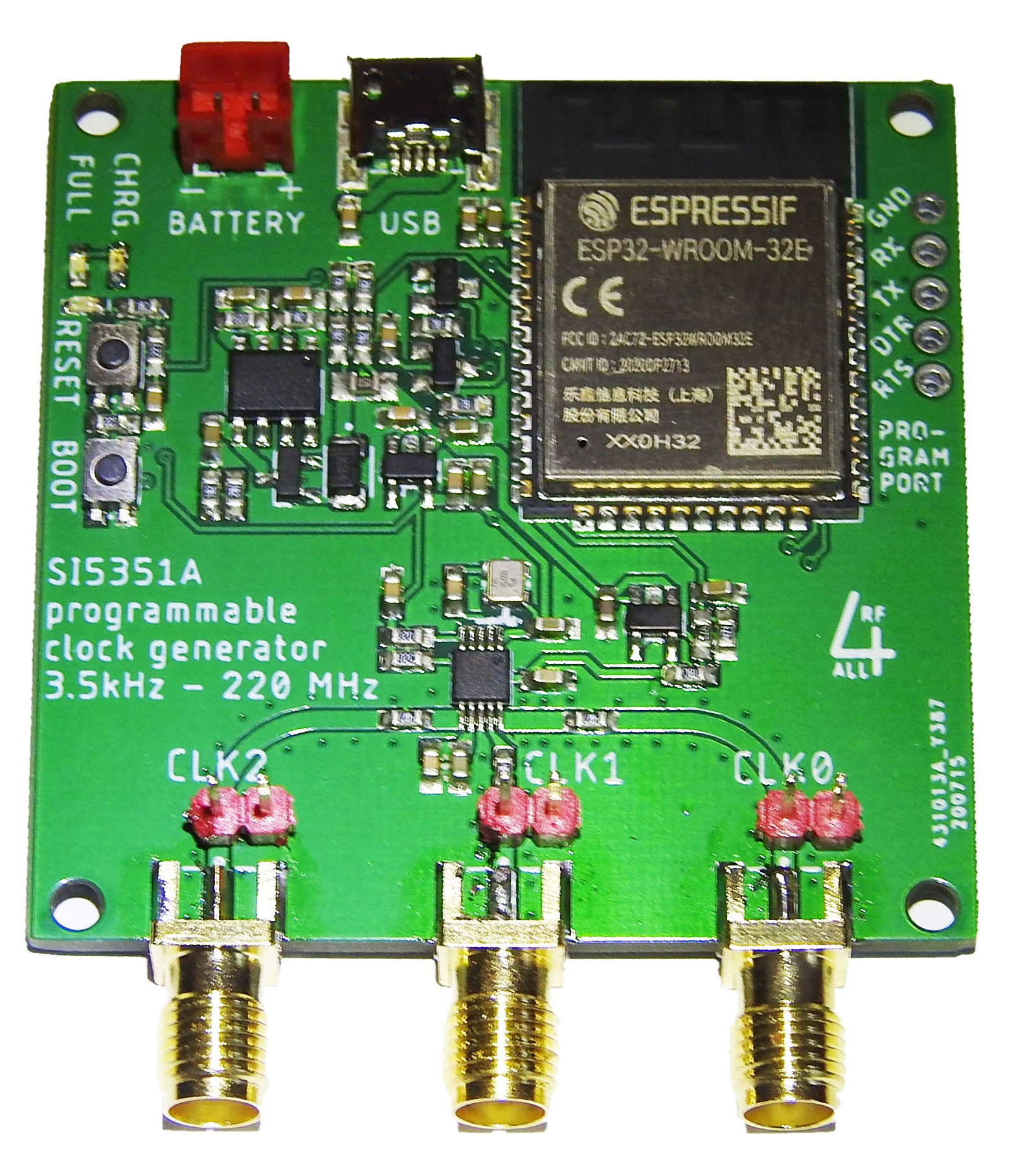
Figure 2 shows the SI5351A Wifi board. Inputs and outputs are:
• Battery connector (JST-PH type) for connecting a 3.7V LiPo battery.
• micro USB connector for USB power supply cable.
• RESET button for resetting the board
• BOOT button. This is not being used.
• SMA output connectors for CLK0, CLK1 and CLK2
• Program port. This is not being used
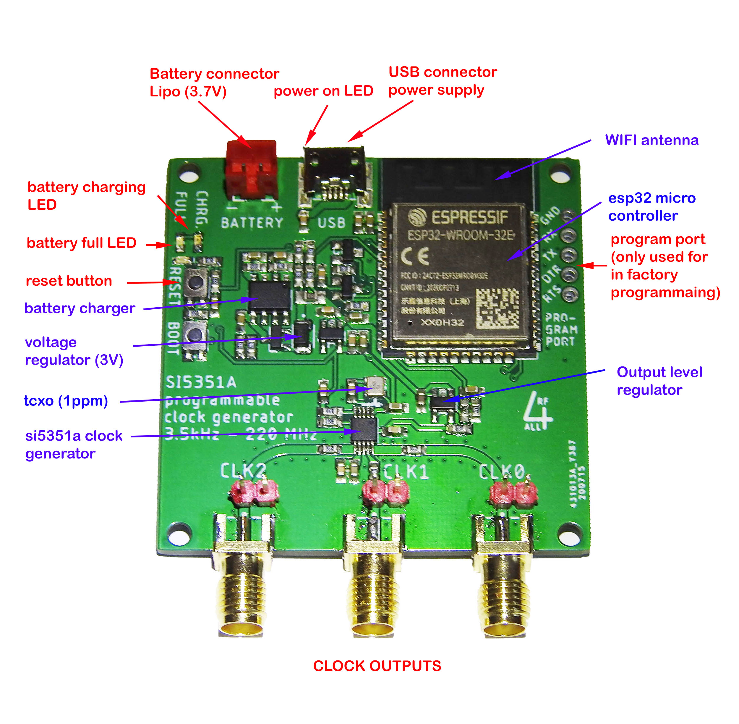
Figure 2. the SI5351A WIFI board.
The main components on the board are the ESP32 microcontroller and the si5351a clock generator. The ESP32 microcontroller is pre programmed. It contains the firmware that reads and writes the SI5351A registers. It contains the server software that enables WIFI communication and allows the user to communicate via a internet browser. It also measures the board's supply voltage and current consumption. This can be monitored with the test software.
Specifications can be found in table 1.
| TABLE 1. SI5351A BOARD SPECIFICATIONS | |
| Number of Clocks | 3 |
| Clock frequency range | 3.2 kHz till 200 MHz |
| Clock frequency resolution |
1 Hz (frequency range: 3.2 kHz - 31 MHz) 5 Hz (frequency range: 31.000005 MHz - 146 MHz) 10 Hz (frequency range: 146.000001 MHz - 200 MHz) |
| Clock Frequency stability | 1 ppm, based on temperature controlled clock oscillator (TCXO). |
| CLK 0, 1,2 output level | 1.2V, 1.8V, 2.5V and 3.3 V (software selectable). DC coupled. |
| CLK 0,1,2 output impedance | 50 ohms |
| CLK 0,1,2 maximum output current | 20 mA |
| Power supply |
Supply voltage: 3.3 till 5.5 Volt Current consumption: 130mA +/-10% (all clock outputs off), 180 mA +/-10% (all clock outputs on and 50 ohms loaded) Connector type: micro USB, LiPo JST-PH |
| Voltage and current monitor |
power supply voltage: 3 till 5.5 Volt, 10 mV resolution supply current into 3 Volt regulator: 0 till 800 mA, 5 mA resolution |
| Communication | WIFI mode (STA) 2.4 GHz, Hotspot mode (AP) 2.4 GHz |
| Battery charger | Maximum battery charge current: 800 mA. Maximum LiPo battery capacity: 3600 mAh. |
| Operating temperature | -25° ... 80° Celsius |
| Dimensions | Dimensions: 50 mm x 50 mm x 11 mm |
| Weight | 13 grams |
4. SI5351A software and Graphical User Interface
The test software allows the user to control the SI5351A parameters and read or write the registers, see table 2 for the parameters that can be controlled. All parameter settings will be stored in the cache of your browser. If you close and re-open the web page, settings from your previous session will be restored.
| TABLE 2. TEST SOFTWARE - CONTROL PARAMETERS (please check the SI5351A datasheet for details.) |
|
| FREQUENCY | Frequency for each clock can be set between 3.2 kHz and 220 MHz. |
| PHASE | Initial phase offset for each clock can be selected. |
| OUTPUT LEVEL | Output logic level can be set for all clocks simultaneously at 1.2, 1.8, 2.5 and 3.3 Volts |
| OUTPUT DRIVE | Output drive for each clock can be set at 2, 4,6 and 8 mA. Low output drive reduces slew rate and frequency harmonics. |
| OUTPUT ENABLE | Each clock output can be enabled (output power on) or disabled (output power off) |
| INVERT | Each clock output can be inverted. |
| PLL | For each clock PLL A or PLL B can be selected. PLL A and PLL B are not synchronized. |
| SPREAD SPECTRUM | Spread spectrum can be enabled or disabled. If enabled it will apply to all clocks simultaneously. Down spread and center spread can be selected. |
Control of the buttons is with mouse or touch. Pages can be swiped left/right. The following chapters describe how to use the software in more detail.
4.1 HOME page
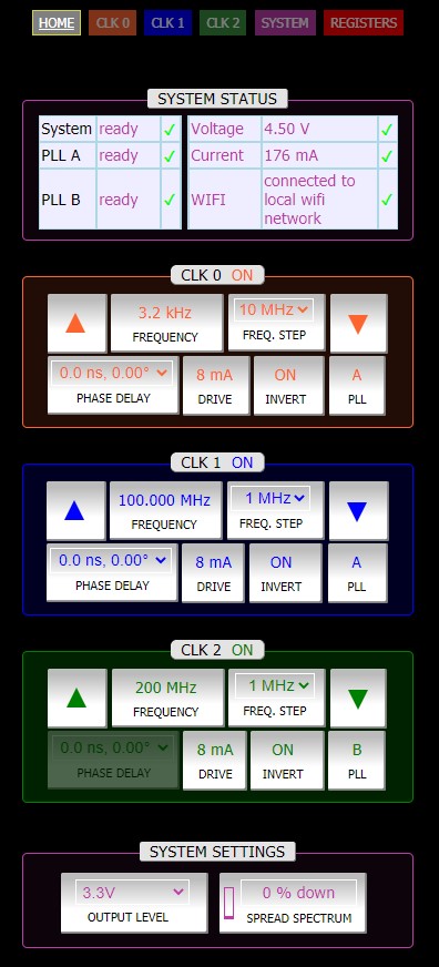
Figure 3. HOME page
On the HOME page there are 5 boxes:
• SYSTEM STATUS reports the health of the si5351a chip, the board's voltage, board's current consumption and connection status.
All boxes should be ticked ✔. A red X indicates an issue.
If the PLLA or PLLB is marked X the PLL is out of lock, resulting in an instable output VCO and output frequency.
• Inside the CLOCK boxes the user can control the individual CLOCK parameters.
To power on/off a clock, toggle the ON/OFF button on top of a clock box.
• Inside the SYSTEMS SETTINGS box the user can control the output level and spread spectrum. Both settings
will affect all clocks simultaneously.
4.1.1 Frequency control
Press the FREQUENCY button to enter a frequency value.
To change from MHz to KHz unit, toggle the unit button (showing MHz or KHz) at the top right of the key pad.
Press the FREQ.STEP button to set the frequency step. This button works in combination with the arrow up and down buttons.
Pressing the arrow button will change the frequency with the FREQ.STEP value.
If you keep the arrow button pressed the frequency will automatically keep changing two times a second.
4.1.2 Phase control
Phase delay can be set for each clock.
The phase values that can be set depend on the frequency of the internal si5351a Voltage Controlled Oscillator (VCO).
The VCO range is between 600 and 900 MHz. The phase can be calculated as follows:
Phase delay (seconds) = n / ( 4 x Fvco) , n=0...31 (the user can select)
Phase (degrees) = n x 90 x Fout / Fvco, Fout is the desired output frequency
An example. With Fout = 80 MHz and Fvco=800 MHz the Phase is: n x 9 degrees.
With Fout =8 MHz and Fvco=800 MHz the Phase is: n x 0.9 degrees.
The software will calculate the list of available phase values for each frequency.
If you wish to have two clocks having a different phase relative to each other, e.g. CLK0: 0 degrees and CLK1: 90 degrees,
make sure that both clocks are on the same PLL. PLLA and PLLB are not synchronized, so they will have an unknown phase between them.
The si5351a does not allow to set a phase for frequencies above 146 MHz. The phase button will be disabled in this frequency range.
4.1.3 PLL
The si5351a has two internal PLLs, PLLA and PLLB, and two internal VCOs. Each PLL controls one VCO. PLLA and PLLB are not synchronized.
Clocks that share the same PLL also share the same VCO. Their VCO frequencies are the same and they are synchronized.
For example: Set CLK0 to PLLA, CLK1 to PLLA and CLK2 to PLLB. Then CLK0 and CLK1 share the same PLL and VCO.
You can set a phase difference between these 2 channels. CLK2 runs independent from CLK0 and CLK1 since it is on another PLL and VCO.
4.1.4 Output control
OUTPUT LEVEL: The user can set the Clock output logic level voltage with the OUTPUT LEVEL button between 1.8 Volts and 3.3 Volts.
All Clocks will have the same level.
DRIVE: Select this button to control the output current drive. This affects the rise and fall time of the Clock signal.
Choose a low value for the lowest amount of harmonics.
INVERT: Set this button to invert the Clock signal (180 degrees phase shift).
4.1.5 Spread spectrum
Use spread spectrum to allow the Clock to jitter or fluctuate around its set output frequency.
This option can be used to reduce Electro Magnetic Interference (EMI). Typically a reduction of 20 dB can be achieved.
You can select 'center' or 'down' spread spectrum. 'center' means that the jitter is symmetric around the base frequency.
'down' means that the jitter range is below the base frequency.
To change from 'center' to 'down', toggle the unit button (showing %center or %down) at the top right of the key pad.
Select a value of 0% to disable spread spectrum.
Spread spectrum will be set for all clocks simultaneously.
4.1.6 Setting frequencies above 100 MHz
Above 100 MHz all clocks that share the same PLL must have the same frequency. If this is the case a 'lock' icon
will be shown inside the FREQUENCY button.
If you wish to set two different frequencies, both above 100 MHz, then use PLL A for one clock and PLL B for the other clock.
It is not possible to set 3 different frequencies that are all higher than 100 MHz.
4.2 CLK0, CLK1, CLK2 page
On the CLK0, CLK1 and CLK2 page, see figure 4, the user can control the parameters for one clock.
The buttons are the same as on the HOME page.
The CLK page also displays the intermediate calculations, the si5351a VCO frequency (Fvco) and the si5351a R output divider value.
Intermediate calculations are used to calculate the register values required for a certain frequency.
Please refer to the si5351a datasheets for more information.
The following formulas apply:
Fout = Fvco / [(a2+b2/c2) x R]
Fvco = Fclk_in x (a1+b1/c1)
Fout is the clock output frequency. Fclk_in is the reference clock connected to the input of the si5351a.
It is a 25 MHz oscillator.
The software does all the calculations according to the si5351a datasheet.
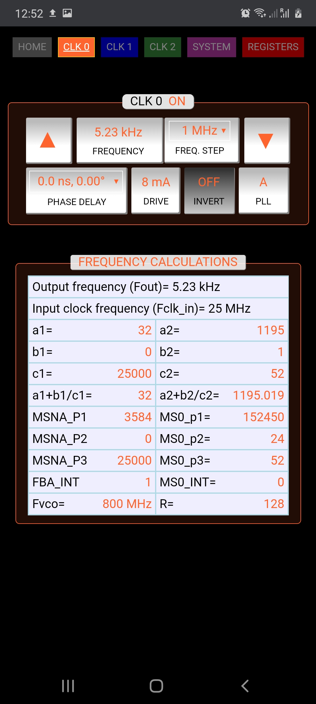
Figure 4. CLK 0 page
4.3 SYSTEM page
The SYSTEM page, see figure 5, can be used to connect the board to WiFi or hotspot. In addition it shows the Spread Spectrum
calculations at the bottom. Consult the si5351a datasheets for more information.
Check chapters 5 or 6 for making a WiFi or hotspot connection.
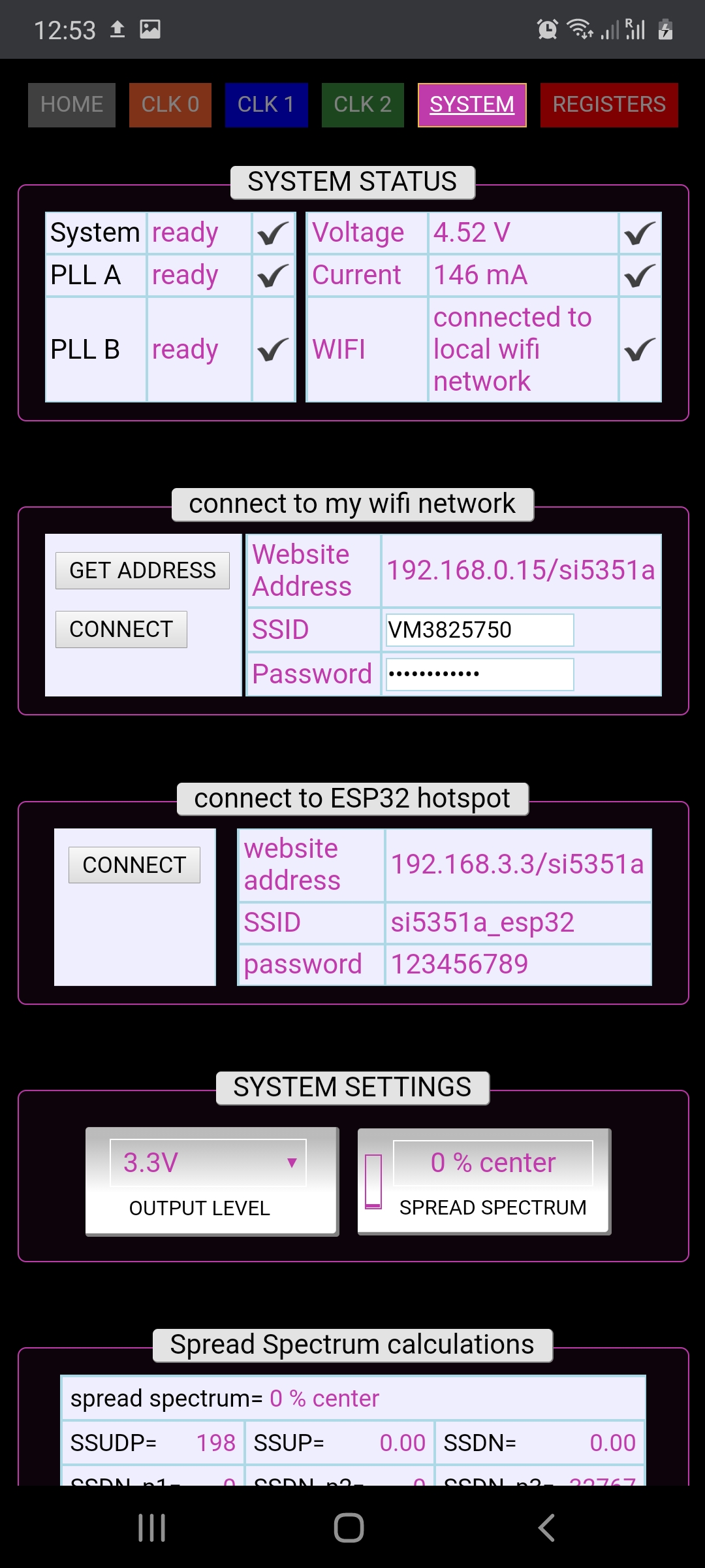
Figure 5. SYSTEM page
4.4 REGISTERS page
The REGISTERS page, see figure 6, shows all register values used for programming the si5351a. There are 183 registers. About half of them are used to control the si5351a. The other registers are used for other si5351 types or are not in use. The register values are updated in real time. The user can use these values for your own application. Please check the si5351a data sheet and application note AN619 (Manually generating an si5351 register map) of Silicon Labs for additional information.
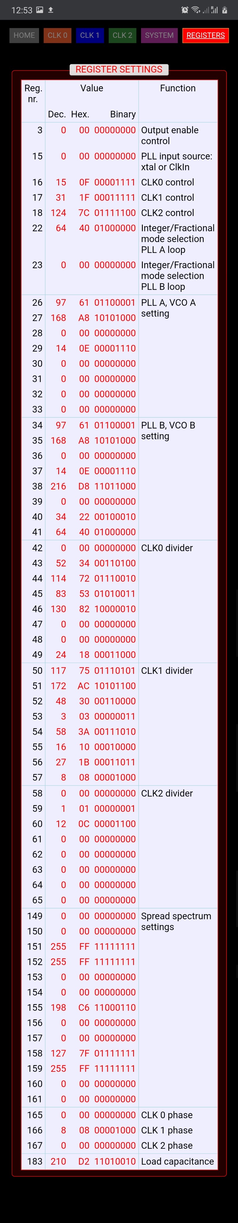
Figure 6. REGISTERS page
5. Connecting to the SI5351A board in hotspot mode
The SI5351A board has an active built-in hotspot. A hotspot connections allows you to communicate with the board privately and without the need for a WIFI network (see figure 7). To connect your smart device or PC to the hotspot take the following steps:
| 1 | Power on the board. |
| 2 | On your smart device or PC select the hotspot network of your board: 'SI5351A_101'. In some cases it might take a while before the board is detected. In that case please re-open or refresh the network selection page. |
| 3 | Enter the network security key / password: 123456789 |
| 4 | After a few seconds you should be connected to your board. Please note that your smart device or PC might ask you if you want to stay connected without internet. In that case answer YES. |
| 5 | Open your preferred web browser and visit the following page: 192.168.3.3/si5351a The SI5351A web page will show up. You can now start controlling your board. |
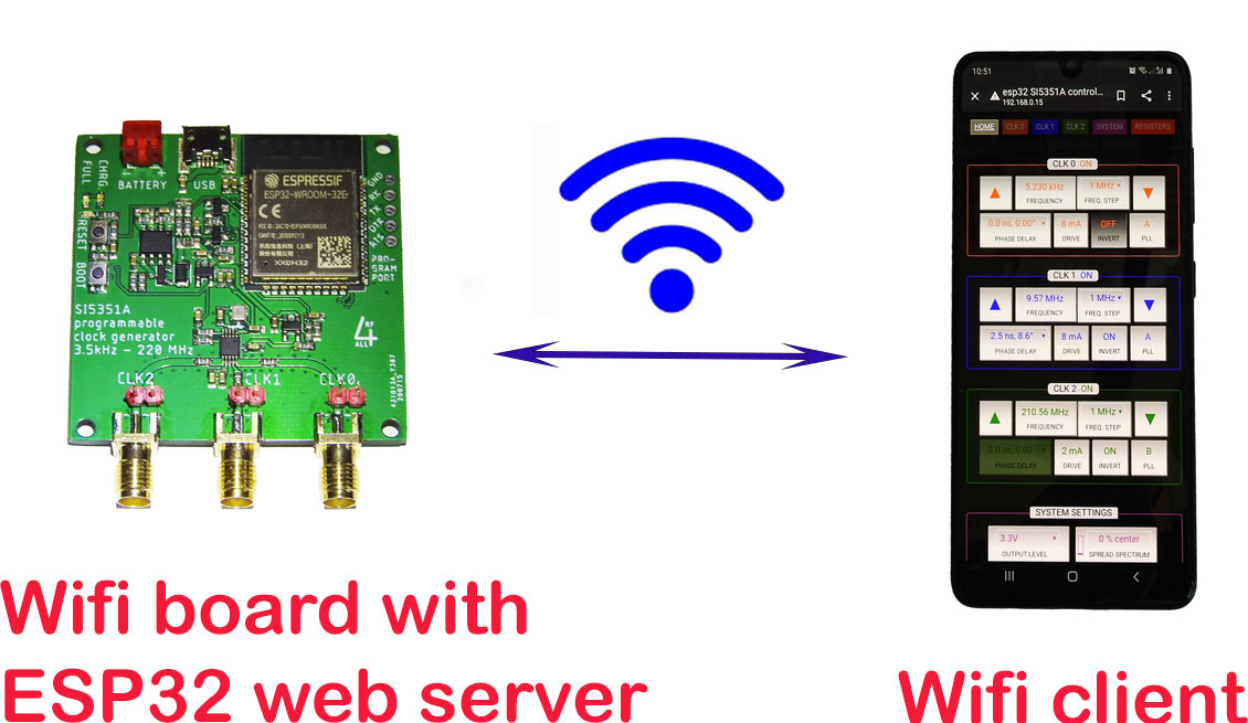
Figure 7. Hotspot connection
6. Connecting to the SI5351A board through WIFI
The board can be connected to your local WIFI network, see figure 8.
The advantage of connecting to WIFI, compared to the hotspot mode, is that you have access to internet.
If you have previously setup a WIFI connection and like to re-connect simply open the board's web page.
Connection should be made automatically.
It you like to connect your smart device or PC to the board through a WIFI network for the first time,
or to a new WIFI network follow the steps 1..6 below:
| 1. | Power on the SI5351A board. |
| 2. | First connect to the hotspot, following the steps in the 'Connect to hotspot' section above. |
| 3. | Once connected to the hotspot select the SYSTEM page. Then go to the 'setup WIFI' section. Type in the SSID and password/network key of your WIFI network. Then press 'GET ADDRESS'. |
| 4. | After a few seconds the WIFI website address will show up. Make a note of it. |
| 5. | Now go the wireless/network settings page on your smart device or PC and connect to your WIFI network. Then, in your internet browser, open the WIFI website address from step 4. |
| 6. | After a few seconds you should be connected to your board and the web page opens. . |
The board will store your WIFI details. When you start a new session the board will automatically try to re-connect to your WIFI network.
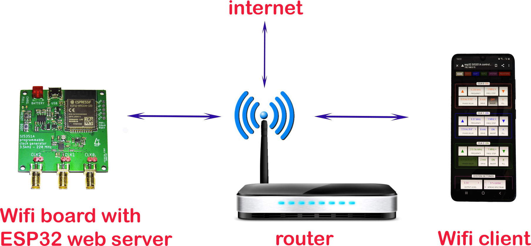
Figure 8. WIFI connection
7. Troubleshooting
CONNECTIVITY
If your smart device or PC disconnects from the board, or the board is unresponsive, please do the following:
• Reset the SI5351A board and make sure it is powered on (blue LED on). Wait 8 seconds.
• Refresh your browser page. You will then automatically re-connect
PLL UNLOCKED
If the PLLA or PLLB is marked X the PLL is out of lock, resulting in an instable VCO and output frequency.
This may happen if the output frequency is above 144 MHz and the output current exceeds 20 mA.
To resolve this you can lower the output DRIVE to 4 or 6 mA.